Main Content Area
Electronic Properties
of Materials - Physics of Semiconductors

Learning Goals:
- Basic properties of intrinsic semiconductors - Carrier Concentration etc.
- Extrinsic Semiconductors
- Semiconductor Band Engineering
- Semiconductor Interfaces
- Semiconductor - Semiconductor Homojunction
- Metal Semiconductor Junctions
- Semiconductor-Semiconductor Heterojunctions
- Semiconductor Devices
- Light Emitting Diode
- Solar Cell
- Transistor
- Bipolar Junction Transistor
- Field Effect Transistor
What are Semiconductors?
In the previous sections, we have found that some materials will not conduct electrons at absolute zero temperture, however, conductivity increases as the temperature is increased. This is the so called class of materials called semiconductors. The valance bands and the conduction bands are shown for metals semiconductors and Insulators in the following figure.
In semiconducting materials, the highest occupied energy level (valance band maximum) and the lowest unoccupied energy level (conduction band minimum) are separated by an energy gap. At a finite temperature, electrons from the valance band thermally excited to conduction band, thus the conductivity increases.
In this lesson, we will discuss about different families of semiconductors, properties of intrinsic semiconductors, properties of extrinsic semiconductors, and semiconductor devices.
******* Missing Some materials here ******
Semiconductor Interfaces
So far, we know the concept of defects in semiconductors. We know how to sketch the electronic band structure of p- and n- type semiconductors. Semiconductor devices are usually made at the junctions or interfaces between semiconductors.
Semiconductor-Semiconductor Homojunction - (p-n Junction):
p-n junction, which is also called the rectifier is the most simplest form of a semiconductor junction. p-n juncton means a region where a p- and n- doped regions meet. The whole junction can be made of the same crystalline material, in which case it is called a homo-junction. It is also important to understand the junctions made at differently doped materials with different crystalline order, are called heterojunctions. Heterojucntions are extremely important in semiconductor device industry. We will discuss the heterojunctions at a later lessons. p-n junction can be made of a single crystalline material with differently doped two sides.
Usually, the junctions are graded, which means that the majority carrier concentration gradually decreases from one side to the other. However, theoretically we consider an abrupt junction.
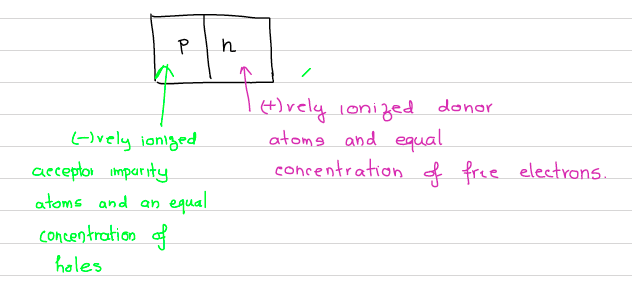
- Acceptor impurity atoms are incorporated into one part to produce a p-region, where majority carriers are holes.
- Donor atoms are doped in the other part ( the n-region) where the majority carriers are electrons.
- Minority carriers present in both sides.
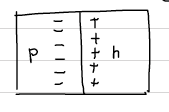
At the moment the junction is prepared, there are majority electrons in n-side and majority holes on the p-side. In another words, if there are electrons in p-side, they are only coming from thermal excitation (which are minority carriers). The electric field is zero everywhere, because the charges of the free carriers are balanced by the charges in the ionized impurities. This situation is however not in an equilibrium. The moment the junction is formed, the charges begin to diffuse: Electrons from n- to the p-region. The holes diffuse from p- to n-region.
The diffusion will not continue indefinitely. Because the contact potential will limit further movement of charge carriers.
As electrons diffuse to the p-side, The electrostatic potential of the junction can be depicted as following:
At the equilibrium, the total chemical potential across the crystal is a constant across the junction. Due to the built-in electric field which created as a result of the charge diffusion, stops further movement of the majority charge carriers. Or else, electrons from n-side see a potential step to cross to the p-side. This potential step can be drawn by considering the alignment of Fermi energy across the barrier. This is called the band bending. Basically a way of representing the built-in-potential or the contact potential at the interface. Band bending is a very important concept to understand. If you understand it right at this most basic level, it will be useful to apply for other semiconductor devices.
p-n junction itself is a very important device component called a rectifier or a diode. Following we will breifly discuss its rectifying properties.
p-n junction in an external voltage (Note that the mathematical equations will be added at the next phase of this website)
Forward Bias:
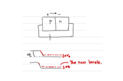
Let's think about the situation, when you connect the p-side to the positive terminal and the n-side to the negative terminal of a external battery.
As a result of the bias voltage, the energy levels of n-region raises. In other words, the applied voltage is opposite to the contact potential. Applied potential supports the motion of the charge carriers. That means, the current increases when you increase the voltage. The I-V characteristics of a p-n junction is shown below.
This is called the forward biasing.
Reverse Bias:
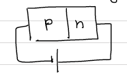
Now if we switch the terminals of the battery as follows: p-to negative end and n- to positive end of the battery, the external voltage act in the same direction as the contact potential. That is, the external potential enhances the effect of contact potential, which is the limitation of the motion of majority carriers. This is called the reverse biasing of the p-n junction. Reverse bias support the motion of the minority carriers. However, current does not increase, as the concentration of charge carriers is limited. That is why p-n junction is called a rectifier. It carries current in one direction, and does not carry a significant current in the opposite direction.
Semiconductor Band Engineering
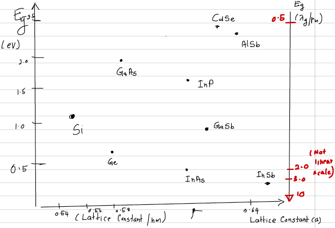
p-n junction (rectifier or a diode) is the most basic element of semiconductor devices. Many other devices are made at the semiconductor heterojunctions, that is at an interface of differently doped different crystalline materials. In order to design devices, we need a semiconductor materials with range of electron band gaps. Also in order for the materials to be grown on top of the others, the lattice parameters are important. Such a wide range are not available in naturally existing semiconducting materials. For example, following graph shows the electron band gap and lattice constants of some semiconductor materials.
It is clear that, we dont have a wide range of bandgaps and lattice constants in naturally existing semiconducting materials.
Si and Ge are elemental semiconductors. There are compound semiconductors. Let's talk about binary compound semiconductors su ch as
- II - VI semiconductors such as ZnS, CdS, ZnSe, CdSe
- III-V semiconductors such as AlP, GaAs, InSb, GaN
- IV-IV semiconductos such as SiC, SiGe
Still, the naturally existing semiconductors provide you with a limited number of energy gaps.
It is important to artificially design materials that are suitable for particular applications. Semiconductor alloys are an example for such artificially created materials.
Semiconductor Alloys:
Two semiconductors are combined to get a artificially engineered material with an intermediate band gap and intermediate lattice constant.
AlGaAs: (Known as Al gaas)
GaAs is a direct bandgap semiconductor, and AlAs is an indirect bandgap semiconductor. These two can be combined to make a solid solution over the entire possible region that is to make AlxGa(1-x)As for x changes between 0 and 1.
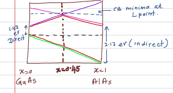
x=0 and x=1 represent the end materials GaAs ad AlAs respectively. The alloy becomes an indirect bandgap material for x=0.45. The details of the changes in the bandstructure of the material is shown in the following figure.
Two important things to notice in these ternary compound semiconductors are the variation of the electronic band structure and variation of the lattice constant. In fact, as we willdiscuss later, both lattice constant and the bandgap are important for designing heterostructure devices.(Please note these images are temporary.... Will have the completed figures soon )
The lattice constant of an alloy is usually given by linear interpolation of its constituents. This is given as Vergard's Law.
For example the lattice constant of AlxGa(1-x)As is given by:
It is important to note that, within the whole range, the total change in the lattice constant is less than 0.15%. Therfore it is possible to gro layers of GaAs and AlAs or any other intermediate alloys on top of one another without a significant stress.
Electronic bandgap of GaAs is 1.42 eV (which is direct) Electronic bandgap of AlAs is 2.17 eV (which is indirect) In the above diagram, x=0 is represent pure GaAs. x=1 represent pure AlAs. In the above figure, line connects between AlAs and GaAs represent the continuous solid solution of AlGaAs. Solid line represent a direct ternary alloy and dashed line represents the indirect bandgap ternary alloy. You can clearly see a indirect-direct transition as the GaAs content increases. We can get a detailed understanding of the indirect-direct crossover by analyzing the variation of band extrema of the band structure.
Detailed of Indirect-Direct crossover of AlGaAs:
Basically the electronic band structure is characterized by two local minimas of the Conduction band, particularly at Gamma point and L point. Relative difference between the CBM's at Gamma point and L point are very sensitive to the AlAs content, that is x.
As we increase x, the valance band maxima changes. (Drawn in Green)
As we increase x, the minimum of the CB at the Gamma point change (Drawn in Blue) CB minimum at the L point also changes.
What matters is the relative difference between the CBM at Gamma point and CBM at L point.
All these changes occur almost linearly as a function of x. Direct-Indirect transition occur as x=0.45. (Ref: The Physics of Low-Dimensional Materials by John Davies )
Semiconductor Interfaces:
Previously we have discussed about one type of semiconductor interface: p-n junction or a rectifier or a diode. We have also discussed how to engineer electron bands of semiconductors. The band engineering is important because we will them have a range of Eg values with a range of lattice constants. Lattice constant is as important as the Eg in semiconductos as lot of devices are made at heterojunction interfaces, that is interfaces at differently doped different crystalline materials. Depending on the electronic band structure of component materials, these junctions show completely different electronic properties. Here we talk about some important two other semiconductor-related junctions.
We are going to discuss about their band alignments.
- Semiconductor-Semiconductor Heterojunction
- Metal-Semiconductor Junction
Semiconductor-Semiconductor Hetero Junctions:
One semiconductor can be grown coherently on another. Not all combinations will work, for such an epitaxial growth. But you can find some combinations. In a homojunction, electronic properties can be controlled by the level of dopants. Heterojunctions add an extra degree of freedom because the band offsets of valance band and conduction band edge also can be tuned. One good example of a heterostructure is GaAs grown on Ge. For both these materials, lattice constant is 5.65 Angstroms. Both lattice structure are diamond type. It in fact looks like the same crystalline structure, where atomic occupancy changes at the interface. However their band structures are different: 0.67 eV for Ge and 1.43 eV for GaAs. The changes in the bandgap at the interface is the root for device engineering in a heterostructure.
OK.... In order to draw these two band structures together, we need one more information, that is a common level for both materials, which is given by work function.
Workfunction: The workfunction W of a uniform surface of a material is defined as the difference in potential energy of an electron between the vacuum level and Fermi level. The vacuum level is the energy of an electron at rest at a point sufficiently far outside the surface so that the electrostatic image force on the electron can be neglected.
Some exapmles: Cu (100) -> 4.59 eV
Cu (111) -> 4.48 eV
Work function can be experimentally evaluated and also can be calculated theoretically.
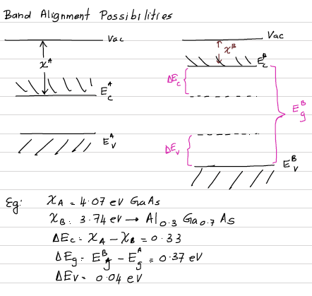
Let's consider an example: GaAs/ Al(0.3)Ga(0.7)As heterojunction. Electron affinity of GaAs and Al(0.3)Ga(0.7)As are 4.07 eV and 3.74 eV respectively. The electronic band gap of GaAs is 1.43 eV and electronic bandgap of Al(0.3)Ga(0.7)As is 1.80eV.
Draw their electronic band diagrams together. Not for a junction. Just draw the individual band structures in the same figure.
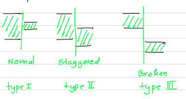
In general, the relative alignment of the conduction band and valance band edges can have several possibilities.
Now knowing how to draw two individual band structures together, we can go ahead and start plotting the band structures at an interface. We will consider a n-N heterojunction (Following Kittel)
n-N HetreoJunction:

