 |
 |
Research Interests
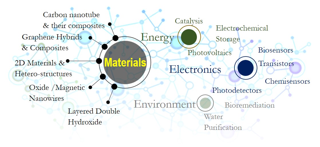
It is envisioned that the field of nanomaterials and nanotechnology will go through a tremendous expansion and will hold immense potential for providing advanced scientific and technological solutions that will have significant societal impact. These materials have shown significant promise in revolutionizing the energy, environment and electronics sectors. Nevertheless, for impacting human life through innovative energy storage/generation technologies as well as nanoelectronic device applications materials with desired properties and with functionalities compatible with present day structural elements of energy utilization processes and future energy technology concepts are needed. Keeping this as the central theme, in the past few years we have developed a strong research program which focuses on utilizing nanomaterials in a variety of applications ranging from energy storage and generation to several other applications in micro/nanoelectronics. Our research interests and some of our current ongoing projects are listed below.
Nanoscale Materials and Structures
Many applications that will ultimately utilize macro architectures fabricated using nanostructures as their primary building blocks. It is envisioned that these architectures (for example free standing carbon nanotube films/fibers, graphene membranes, thin atomic layers of Boron Nitride and Molybdenum Disulphide, magnetic and oxide nanowires etc.) will possess superb properties, such as high specific surface area, high strength, low density, and excellent dielectric as well as electrical properties that will make them potential engineering materials for developing several applications. These could include electrochemical energy storage, efficient catalysts, active components in electronics etc. For these reasons, there is a continual search for novel materials and their synthesis methods that are capable of producing these nanomaterials in large scale. As such, expertise in simple innovative routes for discovery, design and bulk production of several functional nanomaterials is essential. We have developed such expertise in nanomaterials growth & characterization.
Electronic Transport
Mesoscale/Nanoscale materials, due to their unique structure-property correlations, hold a significant promise in discovery of new scientific phenomenon as well as advanced technology development. For example; electron transport investigations in nanoscale systems, in recent times, have provided insights into very exciting and rich physics related to fundamental charge transport behavior in nanoscale systems. As lateral sizes of various materials head below a few tens of nanometers, their electrical properties get affected by quantum confinement effects. Certain key transport parameters, such as number of quantum channels, disorder density (or, inversely, the mean free path), and e-e interactions play a strong role in determining the electronic properties of these nanoscale materials. For example carbon nanotubes are quasi one-dimensional conductors, and very often tend to be defect free compared to metal wires of the same dimensions. It is for this reason, that electron transport in nanotubes is often ballistic, and contact resistance at the electrodes dominates the channel conductance. Similarly, in graphene 2D Dirac like electronic excitations as well as tunable electronics in other 2D van der Waals layer systems, Quantum Materials etc., make them ideal candidate for studying fundamental electronic processes at nanoscale.Investigations in order to understand the interplay of charge, spin, and lattice, at different thermal energy scales as well as under several enviornments are being carried out. It is expected that extremely interesting and rich physics, both at room as well as low temperatures, will be exhibited by these systems.
Light Matter Interaction
Optical functionality is one of the most coveted property of modern day semiconductors and hence understanding the physics of light matter interaction becomes a key to tune, control as well as discover novel phenomenon in novel materials. In recent times investigation of electronic and optoelectronic properties of 2D layered systems (such as MoS2, WS2, MoSe2, BN, InSe) and their heterostructures have gained tremendous attention. This is due to the fact that several of the layered transition metal dichalcogenides possess band gaps in the range of 1 to 2 eV and a transition from an indirect gap in the bulk to a direct gap in a monolayer metal dichalcogenides. In this context, single and few layers of MoS2 have presented itself as a system with high electron mobility, rendering them as potentially useful active elements in thin film transistors. These discoveries, along with the fact that single layer MoS2 is a direct band gap materials (~1.8 eV) in contrast to its bulk counterpart (n-type semiconductor with an indirect band gap of ~1.3ev) has led to the investigations of electrical and optoelectronic properties of single layer MoS2 transistors. Tunability in optical responses by controlling the layer thickness in these materials make them extremely viable for several optoelectronic applications as well. This has led to the possibility of several interesting scenarios related to light matter interaction in these materials.
Energy Storage & Conversion
The ongoing energy crisis and the need for commercially viable clean energy sources have presented itself as one of the foremost challenge of 21st century. A continual search for materials and technology that can provide durable and dependable energy storage solutions to assist in attaining energy security is thus in the fore front of scientific/industrial research. In the last decade, realizing the potential of Electrochemical Double Layer Capacitor (EDLC’s) for next generation energy storage solutions US DoE came up with a report outlining strategically important research directions in order to forge a strong knowledge base required to overcome the present scientific bottleneck for realizing the full potential of EDLC technology. EDLC's (also referred to as Super Capacitors and Ultra-Capacitors) are envisioned as devices that will have the capability of providing high energy density as well as high power density. With extremely high life-span and charge-discharge cycle capabilities EDLC's are finding versatile applications in the military, space, transportation, telecommunications and nanoelectronics industries. Some of our research thrust is to understand fundamental properties of materials systems in order to develop technologically viable supercapacitor devcies. Similarly, materials and processes capable of producing paradigm shift in catalytic science through investigations on novel nanostructured materials (non-traditional catalysts) with tailored surfaces and edge states are also crucial for developing alternative energy technologies.